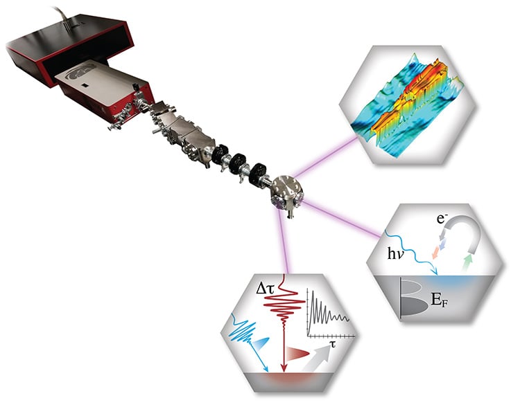


KMLabs QM Quantum MicroscopeTM advanced photon imaging solution is a fully integrated, commercialized platform enabling ultrafast spectroscopy in the EUV range and high-contrast, near surface-to-subsurface imaging at the nanoscale. It enables laboratory-based 2D high contrast imaging of composition and structure, study of mechanical properties of patterned films, deep understanding of materials properties, and functional characterization of spintronic, ALD, 2D, low-density lightweight, energy, space and photovoltaic materials.
Interested in how the Quantum Microscope platform might be useful for semiconductor applications? Check out this video from former JILA graduate student Kathy Hoogeboom-Pot:
By combining the time sensitivity of femtosecond lasers with the spatial resolution of EUV microscopy and diffraction, QM enables a series of techniques tuned for important challenges in research and industry. E.g., for batteries, EUV absorption near the lithium edge provides a microscopic and spectroscopically rich area to understand lithium bonding. For semiconductors, QM provides critical detail on buried and surface nanotopography with unique sensitivity to bonding.
Completely configurable, the QM Quantum Microscope comprises a laser source (EUV and/or VUV), amplifier, beamline tailored to the user’s experiment, and imaging or other analysis workstations that can effectively cover the microscopy/spectroscopy landscape for nano-to-quantum materials.
Applications in development have been performed on KMLabs’ equipped systems as initial proof of concept.
Learn more about these components of a QM Quantum Microscope:
B. Zhang et al. "High contrast 3D imaging of surfaces near the wavelength limit using tabletop EUV ptychography." Utramicroscopy 158 (2015): 98-104
DOI: 10.1016/j.ultramic.2015.07.006
Miao, J. "Beyond crystallography: Diffractive imaging using coherent x-ray light sources." Science 348, 6234 (2015): 525-530
DOI: 10.1126/science.aab0097
Gardner, D.F., et al. "Subwavelength coherent imaging of periodic samples using a 13.5 nm tabletop high-harmonic light source." Nature Photonics 11 (2017): 259-263
DOI: 10.1038/NPHOTON.2017.33