


Applications of Tabletop Extreme Ultraviolet Laser Sources in Nanotechnology and Advanced Manufacturing
Background:
ICALEO's all virtual event was held on October 19 - 20, 2020. KMLabs co-founder and CTO, Henry Kapteyn, gave an update on the imec attolab project. Attolab is a joint collaboration amongst imec, KMLabs, and SPECS aimed at the fundamental studies of EUV photoresists using high harmonic generation coherent light sources at 13.5 - 30 nm with femto- to atto-second time resolution to help understand EUV lithography fundamentals that will be used to manufacture next generation semiconductor chips.
Abstract:
 After more than 30 years of development effort, the microelectronics industry is shifting to the use of much shorter wavelength, extreme ultraviolet (EUV) light at 13.5 nm wavelength for lithographic patterning of nanoelectronics. This is perhaps the largest paradigm shift in the industry since the introduction of photolithography itself, and is fundamentally enabled by advanced laser technologies—for example, the ~100 kW-scale CO lasers used to generate plasma radiation in the EUV.
But this manufacturing transition has not been a simple one. Furthermore, significant gaps in our fundamental understanding still pose serious limitations. For example, EUV light is ionizing radiation -- fundamentally different in its interaction with matter compared with the deep-UV light used previously, yet with some exceptions, the same products are formed. Relatively recently, it has been observed that the “stochastic” variations in exposure, which result in bridges or gaps in patterning, occur far more frequently that would be inferred from photon statistics alone.
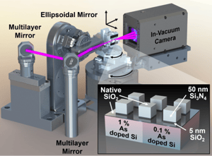
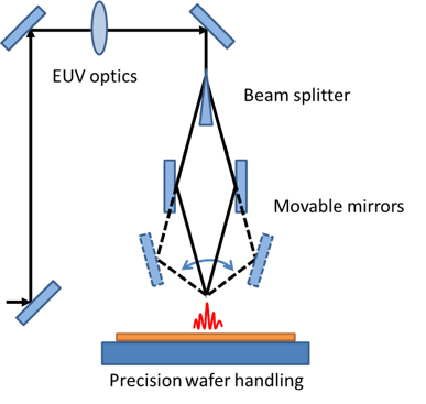
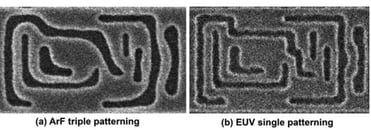 Advanced femtosecond laser technology is now being brought to bear to this problem. The “AttoLab” project being developed by KMLabs, imec (Leuven, BE), and SPECS Surface Nano Analysis GmbH seeks to employ coherent 13.5 nm EUV light, generated through the high-order harmonic generation process, to study the issue of stochastics of photoresist exposure process using time-averaged and time-resolved infrared and electron spectroscopy, EUV radiometry, and coherent diffractive imaging. High-angle interference lithography will allow for small-area exposures with line patterning as dense as ~8 nm pitch, while other beamlines will study exposure dynamics using photoelectron spectroscopy and time-resolved IR absorption. The goals of this project include developing a better understanding of the fundamentals of the EUV resist exposure process using high angle interference lithography. This project is approaching the commissioning stage. Coherent EUV light can also be applied to nanoscopy using coherent diffraction imaging techniques, which allow for unprecedented diffraction-limited resolution in the EUV, which can also be used for EUVL mask review as well as for broader nanotechnology applications. Finally, ultrafast coherent EUV sources are ideal for probing nanoscale mechanical and electronic properties of advanced materials, addressing characterization gaps of current metrology methods.
Speaker Bio:
Henry Kapteyn is a Professor of Physics and CTO of KMlabs, Inc.. He is well known for his work in ultrafast laser technology, the use of intense ultrafast lasers for generating coherent short-wavelength light, and the application of this new "tabletop x-ray laser" light source for both basic science and emerging applications. Prof. Kapteyn is a member of the National Academy of Sciences, and his honors include the 2020/1 Benjamin Franklin Medal in Physics, the RW Wood Prize in 2010, and the Ahmed Zewail Award in 2009.
Won't be able to make it to the zoom meeting live? Don't worry, we've got you covered. Check back soon to replay a recording of the talk and share with your friends!