As semiconductor devices continue to shrink while adopting increasingly complex three-dimensional architectures, accurate characterization of nanoscale features and interfaces has become one of the key challenges in process development and manufacturing. Conventional metrology techniques such as scanning electron microscopy (SEM) and atomic force microscopy (AFM) each provide valuable information but are often limited by throughput, field of view, sample interaction, or their ability to characterize complex three-dimensional structures. Optical scatterometry has therefore become an important metrology technique because it offers fast, non-destructive measurements over statistically relevant sample areas. Extending scatterometry into the extreme ultraviolet (EUV) further improves sensitivity to nanoscale geometry and material composition, making it an attractive approach for future semiconductor process control [1-5].
High harmonic generation (HHG) provides a unique laboratory-scale source of coherent EUV light that combines several capabilities particularly valuable for scatterometry [3,4]:
These characteristics combine to provide a highly flexible EUV source for advanced scatterometry, that have been successfully demonstrated on industry samples [1-5].
The capabilities of coherent tabletop EUV scatterometry using KMLabs’ XUUS source were recently demonstrated by characterizing the critical dimensions of nanoscale gratings [2], as well as by characterizing a two-dimensional periodic semiconductor interconnect structure representative of hybrid bonding applications [5].
Example critical parameters that were extracted for the grating samples include the grating base and mid-line thickness, height, side wall tilt and oxide layer (see Figure). Moreover, these tabletop EUV measurements compared very well with facility-scale critical dimension small-angle soft X-ray scatterometry (SAXS).
In a second example, the copper dishing depth created during chemical mechanical planarization (CMP) was measured. Nanometer-scale deviations can affect bonding quality, making accurate topography measurements essential for process optimization. By performing coherent scatterometry at 29.4nm, the average copper dishing depth was extracted with single-nanometer sensitivity, reporting a value of 2.5 nm.
Most importantly, this study showed that the measurement precision depends strongly on illumination wavelength and the incident angle. Computational optimization identified an optimum wavelength of 13.8 nm for the investigated structure—well within the tuning range of the XUUS. While the optimum wavelength is application dependent, this example highlights how wavelength tunability enables the measurement conditions to be tailored for maximum sensitivity.
These experiments demonstrate that coherent EUV scatterometry can quantitatively characterize nanoscale out-of-plane features on industrially relevant semiconductor structures while maintaining the speed and non-destructive nature expected from optical metrology.
An important advantage of HHG-based EUV sources extends beyond simply generating coherent EUV light. Because the HHG spectrum is tunable, the experimental conditions can be selected to maximize the measurement sensitivity for a particular sample or measurement objective [5].
As semiconductor devices continue to incorporate increasingly complex three-dimensional architectures, metrology solutions must deliver high sensitivity without sacrificing throughput or flexibility. Coherent EUV scatterometry addresses many of these requirements. Tabletop HHG sources provide the combination of high coherence and stability, low beam divergence, broad spectral coverage, wavelength tunability, polarization and easy access needed to enable precision, high throughput, metrology of semiconductor samples.
Although this note discusses EUV scatterometry, the same concepts can be applied to other EUV metrology techniques such as reflectometry and imaging reflectometry [6], highlighting the versatility of coherent HHG sources across a broader range of characterization methods.
Lastly, while this application note focuses on scatterometry, the unique combination of coherence, wavelength tunability, and experimental flexibility offered by HHG sources also makes them attractive for a broader range of EUV and soft X-ray metrology and imaging applications, including overlay metrology.
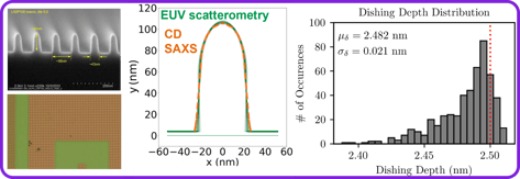
Figure: Example applications in EUV scatterometry, to measure critical dimensions of nanoscale gratings,[2] or dishing depths of interconnects [5].

© Copyright 2018-2024 KMLABS leading in ultrafast All Reserved | Privacy Policy